Amplifier size Increase efficiency Increase current capability Improve the MOSFET thermal efficiency 2. The design goal is to achieve a flat gain over a large bandwidth while achieving the lowest noise possible.

Case Study Analysis Of A Distributed Amplifier By Michael Steer Youtube
Let me try to find it.

. Affect the DA gain flatness. A CMoy pocket amp with a decent but unexceptional op-amp followed by a gang of high-spec PIMETA v2s might well sound better than if the PIMETAs had the same op-amp as the CMoys. BW of DA is limited by BW of G m stages.
Distributed amplifier tutorial I have tried to design some distributed amplifier using the book by Virdee. The quest to build a 50 watt amplifier I began my QRO project by searching my 1998 ARRL handbook for linear amplifier construction projects. One of them An HF 50 Watt Linear Amplifier was a complex schematic that covered two pages.
In that year Percival proposed a design by which the transconductances of individual vacuum tubes could be added linearly without lumping their element capacitances at the input and output thus arriving at a circuit that achieved a gain-bandwidth product greater than that of an individual tube. Of how I worked my way up to a real linear amplifier. The idea is to take a xed g m transistor width W and split it into parallel ngers that are embedded into a transmission line at the gate and drain.
ERROR AMP 3 1 8 4 2 Q1 MOSFET Q2 MOSFET L1 INDUCTOR C1 CAPACITOR R1 LOAD Gate Driver -U1A ERROR AMP 3 1 8 4 2 Q1 MOSFET Q2 MOSFET L1 INDUCTOR C1 CAPACITOR R1 LOAD Gate Driver Vref Load Current Direction Buck Converter Class D Amplifier Fc of LPF is above 20KHz Both current directions ÎInfluence of dead time is different ÎDead time needs to. G m variations with freq. I do have design examples using ADS.
Enhancement of Broadband Amplifiers Narrowband Amplifiers 7 Noise Modeling in Amplifiers 8 Noise Figure Impact of Amplifier Nonlinearities 9 Low Noise Amplifiers 10 Mixers 11 Voltage Controlled Oscillators. EMI considerations Better control of current and voltage transients 3. Noise contribution of G m stage should be low.
In Virdees book they use a chip FET and use wire bound as inductors. The DA stability is compromised when using multi-stage amplifiers as gain stage. I found three examples of linear amplifiers.
The analysis of this circuit is essentially the same as that of an inverting amplifier except that the noninverting input of the op-amp is at a voltage equal to a fraction of V 2 rather than being connected directly to ground. How the package affects the design. Bob is also a prolific designer of audio test equipment including a high-performance THD analyzer and many purpose-built pieces of audio gear.
Basics of 60GHz LNA and PA Design in CMOS 10 of 82 Consequences of short wavelength High path loss For. The theory behind the distributed amplifier is that a number of FETs at least two but more typically four five or six are fed by a periodic structure at the input that. A distributed amp is a clever way to provide enormous bandwidths as much as 100 GHz.
Building Testing a Distributed RF BJT Amplifier The following is a list of parts needed for this part of the tutorial lesson. I dont know this approach will be good up to 10 GHz or not. Both transmission lines need to be properly terminated to see.
From the S-parameter data of the RF BJT at 4GHz you find that Δ 0488 -162 K 1195 Γ S 0872 123 Γ L 0876 61 G Tmax 167dB. 1 2 2 2 2 Line losses per section. If all the resistor values are equal this amplifier will have a differential voltage gain of 1.
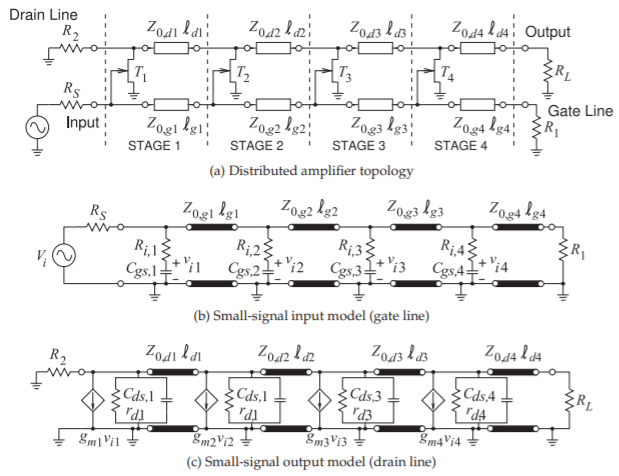
The distributed a mplification method can provide a. On-chip spiral inductors were utilized in on-chip bias circuitry. One transmission line connects the inputs or gates of the devices in a FET based amplifier and is then terminated with a resistor.
Distributed Ampli er v s v o Zd Z g M1 M2 M3 M4 dZ d gZ g g d Z Z g The goal is to convert the lumped ampli er into a distributed structure. G G G Y. The design approach includes the various loss mechanisms inherent in the FET transistor as well as transmission line losses and passive device losses.
The goal is to design a distributed BJT amplifier for maximum gain at f 4GHz. The other transmission line connects the outputs or the drains in a FET based amplifier and provides the output of the amplifier. In Moez 2008 a further design method based on the modified distributed amplification method was proposed.
For designing the differential amplifier accordingly. Design and Simulation of Synthesizers PDF - 15MB 19 Basics of Wireless Communication 20 Performance Measures of Wireless Communication. Assume some specifications such as the Gain Bandwidth Slew-rate Load Capacitance ICMR range etc.
Some distributed amplifiers can operate down to DC as well so they are used as opto-electronic amps. Faculties and often novel design capabilities for a given IC process. DAS works by receiving power from a radio frequency RF source and distributing it over a system.
I have done it for few years. Distributed Antenna System DAS Tutorial Design. High G m value is desired to enhance DA gain.
DAS stands for Distributed Antenna System which is a system that allows for the use of cell phones and other wireless devices in areas that do not have direct access to a cell tower or power source. From the model files in the circuit. The distributed amplifier functions by creating a pair of transmission lines.
A practical design is also illustrated. Index Terms- - Distributed Amplifiers Traveling Wave. Amplifiers with vacuum tubes bipolar transistors and MOSFETs.
Input degernation with distributed amplifier at the upper 3 - dB design frequency of the amplifier Suppose we apply degeneration to make G 11new G 22new max 11 22 2 2111 22 221 2 0 221 2 2 max 21 max 11 0 max 22 0 max in 11 0 out 22 0 11 0 4 4 4 Circuit power gain 1 Maximum sections. Distributed amplifier tutorial I have tried to design some distributed amplifier using the book by Virdee. Design issues in DA gain stages.
The design of the distributed amplifiers was first formulated by William S. The input signal is converted into a pulse width modulated rectangular signal using a comparator. A wasteful but easy and functional way to build such a distribution amp is to buildbuy K1 headphone amps set K of them to a gain of 1 and build an octopous cable.
Microwave Amplifiers made by field effect transistors FET in two different integrated circuits Microwave. Below you can see the block diagram of a basic PWM Class-D amplifier just like the one that we are building. Distributed Antenna System DAS Tutorial Design.
Determine the technology-dependent parameters like V DD threshold voltage of pMOS and nMOS V tp and V tn µ n C ox µ p C ox etc. Consequently the focus of this thesis is upon the application of distributed integrated circuit methodologies towards the realization of a distributed broadband amplifier in a commercial CMOS process technology. Distributed Amplifiers are in two different types they can be selected by considering needs and aim of.
Distributed Ammlifier Oscillator Design Circulator Introduction. Amplifier linearity Decrease switching times Narrow the MOSFET parameter distribution S2 G2 D2S1 G1 D1 TO-220 Full-Pak. He has published numerous articles and papers on power amplifier design and distortion measurement.
This basically means that the input is encoded into the duty cycle of the rectangular pulses.
3 2 Distributed Amplifiers Engineering Libretexts

Pdf Distributed Amplifier A Tutorial Review

Area Reduction Techniques For Full Integrated Distributed Amplifier Sciencedirect

4 Stage Distributed Amplifier Optimised Circuit Download Scientific Diagram
Microwaves101 Distributed Amplifiers

Few Lm317 Voltage Regulator Circuits That Has A Lot Of Applications Voltage Regulator Circuit Electronic Schematics

Shows Schematic Diagram Of Two Way Combined Amplifier Each Way Download Scientific Diagram
Rf Design 16 Practical Power Amplifier Design Part 1 Youtube
0 comments
Post a Comment